


Semiconductor

Yasojima has over 30 years of experience serving semiconductor equipment manufacturers and is the market-leader in Japan.
We
are committed to innovation and efficiency and our experience and engineering expertise in the semiconductor
industry can work for you at every stage of processing.
Yasojima takes a forward vision partnership approach dedicated to providing your company with full-service
manufacturing and strategies to deliver real results.
Physical properties of materials
The semiconductor material is a kind of electronic materials with semiconductor properties. Yasojima Proceed offers a broad range of high-temperature, high-purity materials that provide solutions to critical applications throughout the manufacturing process. Yasojima will work with your organization to quickly develop the right solution for your needs. We can help you identify the critical-to-quality features in your project, define what mechanical and physical properties are key, select the most suitable machining materials, and present manufacturing options to suit your timeline and end-use goal.
Frequently asked properties by semiconductor engineers
・Mechanical properties: creep, fatigue, and impact resistance. ・Thermal characteristics: deflection temperature under load, continuous service temperature, and thermal conductivity. ・Chemical resistance: concentration and temperature. ・Electrical properties: electrical resistance (insulation/conductivity), dielectric rate, and arc resistance. ・Sliding properties: friction coefficient, and PV value. ・Outgas ・Metal elution ・Plasma resistance ・Contact angle (hydrophobic/hydrophilic) ・Dimensional stability
Technology
Complex machinery in the semiconductor industry can benefit from the same advantages our technology brings to other industries, such as improved efficiency, production on demand, and innovative design possibilities. Variation reduction in machining accuracy, shape accuracy such as flatness, microfabrication, thin wall machining of standard parts, complex welding processing, improvement of surface roughness, and burr-free machining are all features machining with Yasojima can bring to your project. As your strategic partner, Yasojima provides innovative machining solutions that give you freedom of design and a seamless transition from prototyping to low-volume production of custom end-use parts.
Best-in-class processing technologies by Yasojima
・High-precision/precision machining ・Welding (PEEK, PPS, etc.) ・Surface finishing (surface roughness control) ・Laser marking ・Identification assembly ・3D inspection/3D measurement (scanner, 3D measuring device) ・Cleanrooms for cleaning and packaging.
Manufacturing
Yasojima can offer innovative solutions to improve the efficiency of your organization’s semiconductor manufacturing processes. Whether it’s the front-end process for dry-type or wet-type equipment or back-end processes for mounting and final inspection, Yasojima has the knowledge and expertise to select the most suitable machining materials, and present manufacturing options to suit your timeline and end-use goal while adhering to strict quality requirements and specifications.
Examples of product adoption
・Exposure/coating equipment ・Etching equipment ・Film deposition equipment (CVD, sputtering, ion implantation) ・Cleaning equipment ・CMP equipment ・Handlers/testers, etc.
Applications
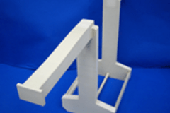
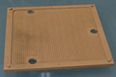
Wafer carrier
| Material | MELDIN® 7001 |
|---|---|
| Size | 150 x 90 x 50mm |
| Why adopt | Plasma resistance, heat resistance, low outgas, cost reduction |
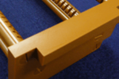
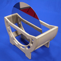
Wafer guide
| Material | PEEK |
|---|---|
| Size | 760 x 425 x 223mm |
| Why adopt | Heat resistance, prevention of chipping and damage of carriers, cost reduction |
Nozzle
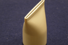
| Material | PEEK |
|---|---|
| size | 45 x 40 x 26mm |
| Why adopt | Chemical resistance, heat resistance, less elution of impurities |
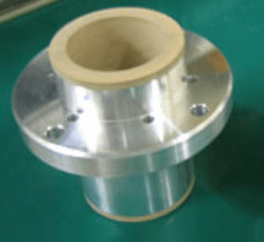
Manifold
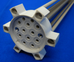
| Material | PEEK |
|---|---|
| size | Φ80 x 430mm |
| Why adopt | Mechanical strength, cleanliness, weldable |
Wafer carrier
| Material | PEEK |
|---|---|
| size | 350 x 200 x 200mm |
| Why adopt | Weldable, chemical resistance, heat resistance, mechanical strength, processing accuracy |
Socket for IC inspection
| Material | Sumika Super® S1000 |
|---|---|
| size | 60 x 60 x 2mm |
| Why adopt | Dimensional stability, less burr |
Bush
| Material | Sumika Super® S300 |
|---|---|
| size | Φ80×Φ68×120mm |
| Why adopt | Reduced noise and motor load by improving slidability |
Quality system
Yasojima has all the systems in place to provide our partners and customers with peace of mind. Yasojima can deliver innovative solutions with outstanding service and support. You can depend on us to adhere to strict quality requirements and specifications, deliver reliable materials, and provide accurate information and best in class technical support.
Quality control system (ISO acquisition)
Yasojima manages traceability throughout our manufacturing processes and can track changes as they occur to keep records up to date.
Business continuity plan (BCP)
Threats and disruptions in your manufacturing processes can result in a loss of revenue, higher costs, and a potential drop in profitability. Because of this, Yasojima operates five high-capacity manufacturing factories across Japan and we are capable of responding to any disruptions experienced by our partners and customers.
Inspection system
Yasojima has variety of specialized 3D scanning and measuring instruments as well as general inspection equipment and can provide an effective and reliable way to acquire accurate 3D measurements of physical objects anywhere.
Cleanroom/Ultrasonic cleaning
In addition to general degreasing, ultrasonic cleaning and clean packaging are available in the cleanrooms installed and maintained at each of our factories.
In addition, Yasojima and its cooperating partner can provide specific cleaning and packing methods depending on your requirements.

- Do you have a question about how Yasojima can help you and your manufacturing processes?
- Can Yasojima recommend a material that provides resistance to chemicals, temperature, vacuum, or voltage?
- Can we tell you about how Yasojima can help you with design, prototyping, or production of your required end-use parts?
We will answer various inquiries such as.
Click here for inquiry form